
GIVE THE PERFECT GIFT
Erin Mills Town Centre Gift Cards are the perfect choice for your gift giving needs.Purchase gift cards at kiosks near the food court or centre court, at Guest Services, or click below to purchase online.PURCHASE HEREHome
Materials and Devices for End-of-Roadmap and Beyond CMOS Scaling: Volume 1252
Indigo
Loading Inventory...
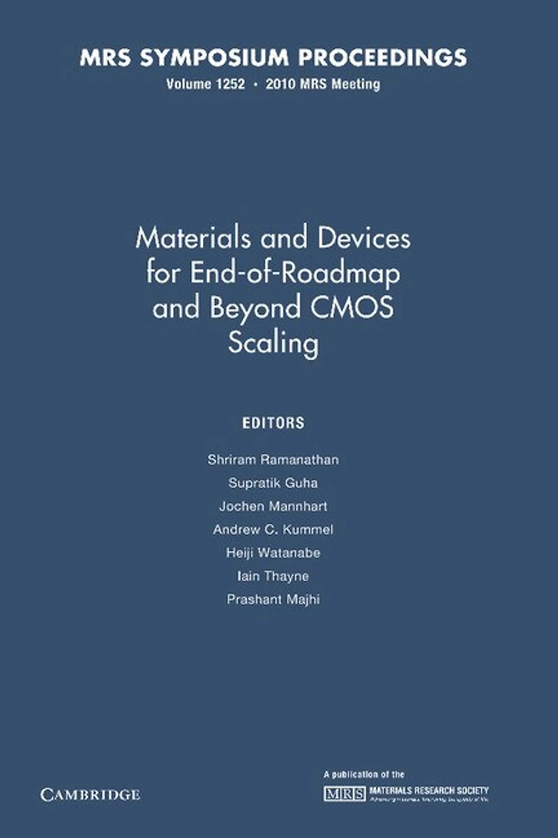
Materials and Devices for End-of-Roadmap and Beyond CMOS Scaling: Volume 1252
Current price: $44.95

Materials and Devices for End-of-Roadmap and Beyond CMOS Scaling: Volume 1252
Current price: $44.95
Loading Inventory...
Size: Paperback
*Product information may vary - to confirm product availability, pricing, shipping and return information please contact Indigo
This proceedings volume contains papers presented at Symposium I, 'Materials for End-of-Roadmap Scaling of CMOS Devices', and Symposium J, 'Materials and Devices for Beyond CMOS Scaling', held April 5–9 at the 2010 MRS Spring Meeting in San Francisco, California. These symposia attracted 106 presentations, of which twenty-two were invited. Historically, scaling in Si CMOS was primarily led by lithography. In the last decade, this situation has been completely revolutionized with the introduction of the likes of copper interconnects, high-k gate dielectrics, metal gates, and strained silicon to meet the demands of the International Technology Roadmap for Semiconductors as the technology generations were reduced beyond 45 nm. As we look towards the end of the roadmap and beyond, the proliferation of potential solutions to meet the necessary performance challenges becomes truly staggering, and has motivated an exponential increase in research in a wide range of emerging materials and devices architectures.
This proceedings volume contains papers presented at Symposium I, 'Materials for End-of-Roadmap Scaling of CMOS Devices', and Symposium J, 'Materials and Devices for Beyond CMOS Scaling', held April 5–9 at the 2010 MRS Spring Meeting in San Francisco, California. These symposia attracted 106 presentations, of which twenty-two were invited. Historically, scaling in Si CMOS was primarily led by lithography. In the last decade, this situation has been completely revolutionized with the introduction of the likes of copper interconnects, high-k gate dielectrics, metal gates, and strained silicon to meet the demands of the International Technology Roadmap for Semiconductors as the technology generations were reduced beyond 45 nm. As we look towards the end of the roadmap and beyond, the proliferation of potential solutions to meet the necessary performance challenges becomes truly staggering, and has motivated an exponential increase in research in a wide range of emerging materials and devices architectures.
You May Also Like






More About Indigo at Erin Mills Town Centre
The largest book retailer in Canada also offers toys, music, home décor, gifts and lifestyle products. What's Inside...Books, Magazines, CD’s and DVD’s, Toys and Gifts, Home Accents, Electronics, Baby’s and Children’s Section, Bath and Body, Kitchen and Bedroom, Stationary Located outside in the exterior plaza.
5015 Glen Erin Dr, Mississauga, ON L5M 0R7, Canada
Find Indigo at Erin Mills Town Centre in Mississauga ON
Visit Indigo at Erin Mills Town Centre in Mississauga ON