

GIVE THE PERFECT GIFT
Erin Mills Town Centre Gift Cards are the perfect choice for your gift giving needs.Purchase gift cards at kiosks near the food court or centre court, at Guest Services, or click below to purchase online.PURCHASE HEREHome
Thin Film Growth Techniques for Low-Dimensional Structures
Indigo
Loading Inventory...
Thin Film Growth Techniques for Low-Dimensional Structures
Current price: $80.50

Thin Film Growth Techniques for Low-Dimensional Structures
Current price: $80.50
Loading Inventory...
Size: Paperback
*Product information may vary - to confirm product availability, pricing, shipping and return information please contact Indigo
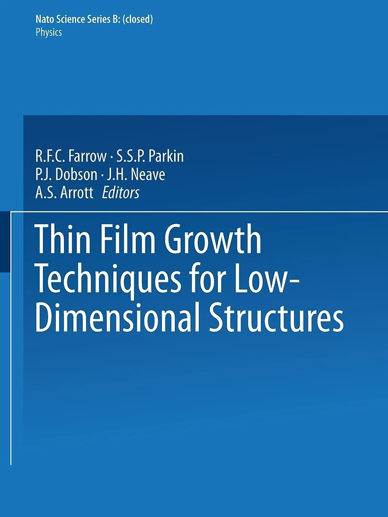
This work represents the account of a NATO Advanced Research Workshop on "Thin Film Growth Techniques for Low Dimensional Structures", held at the University of Sussex, Brighton, England from 15-19 Sept. 1986. The objective of the workshop was to review the problems of the growth and characterisation of thin semiconductor and metal layers. Recent advances in deposition techniques have made it possible to design new material which is based on ultra-thin layers and this is now posing challenges for scientists, technologists and engineers in the assessment and utilisation of such new material. Molecular beam epitaxy (MBE) has become well established as a method for growing thin single crystal layers of semiconductors. Until recently, MBE was confined to the growth of III-V compounds and alloys, but now it is being used for group IV semiconductors and II-VI compounds. Examples of such work are given in this volume. MBE has one major advantage over other crystal growth techniques in that the structure of the growing layer can be continuously monitored using reflection high energy electron diffraction (RHEED). This technique has offered a rare bonus in that the time dependent intensity variations of RHEED can be used to determine growth rates and alloy composition rather precisely. Indeed, a great deal of new information about the kinetics of crystal growth from the vapour phase is beginning to emerge.
This work represents the account of a NATO Advanced Research Workshop on "Thin Film Growth Techniques for Low Dimensional Structures", held at the University of Sussex, Brighton, England from 15-19 Sept. 1986. The objective of the workshop was to review the problems of the growth and characterisation of thin semiconductor and metal layers. Recent advances in deposition techniques have made it possible to design new material which is based on ultra-thin layers and this is now posing challenges for scientists, technologists and engineers in the assessment and utilisation of such new material. Molecular beam epitaxy (MBE) has become well established as a method for growing thin single crystal layers of semiconductors. Until recently, MBE was confined to the growth of III-V compounds and alloys, but now it is being used for group IV semiconductors and II-VI compounds. Examples of such work are given in this volume. MBE has one major advantage over other crystal growth techniques in that the structure of the growing layer can be continuously monitored using reflection high energy electron diffraction (RHEED). This technique has offered a rare bonus in that the time dependent intensity variations of RHEED can be used to determine growth rates and alloy composition rather precisely. Indeed, a great deal of new information about the kinetics of crystal growth from the vapour phase is beginning to emerge.
You May Also Like








More About Indigo at Erin Mills Town Centre
The largest book retailer in Canada also offers toys, music, home décor, gifts and lifestyle products. What's Inside...Books, Magazines, CD’s and DVD’s, Toys and Gifts, Home Accents, Electronics, Baby’s and Children’s Section, Bath and Body, Kitchen and Bedroom, Stationary Located outside in the exterior plaza.
5015 Glen Erin Dr, Mississauga, ON L5M 0R7, Canada
Find Indigo at Erin Mills Town Centre in Mississauga ON
Visit Indigo at Erin Mills Town Centre in Mississauga ON